DVFL2800S
DVFL2800S
The DVFL series of DC-DC converters are designed for high-reliability applications, suitable for military use with an operational temperature range from -55°C to +125°C. These converters feature noise-reducing filters, operate at a fixed frequency of 450 kHz, and include high-speed magnetic feedback and under-voltage lockout to prevent slow start-up issues. They are manufactured in an ISO9001 certified facility and comply with MIL-PRF-38534 and MIL-STD-883 standards.
- High reliability with parallel capability for up to 5 units with current sharing.
- Output voltage trim capability of +10% or -20%.
- Wide input voltage range of 16 to 40 volts per MIL-STD-704.
- Output power up to 120 watts.
- Fault-tolerant magnetic feedback circuit without optoisolators.
- Indefinite short circuit and current limit protection.
- Industry-standard pinout and hermetic package.
- High power density (> 80 W/in³) with custom versions available.
- Compliance with MIL-STD-461 EMC requirements using VPT’s EMI filters.
Absolute Maximum Ratings
- Continuous input voltage: 40 VDC
- Transient input voltage (1 second): 50 volts
- Output power: 120 watts
- Storage temperature: -65°C to +150°C
- Lead solder temperature (10 seconds): 270°C
- Weight: 86 grams
- Input Voltage: 16V to 40V, transient up to 50V.
- Current: Inhibited current ranges from 1 to 70 mA, no load current up to 160 mA.
- Output Voltage: Varies with temperature, maintaining stability across specified ranges.
- Efficiency: Ranges from 80% to 85% depending on the model and conditions.
- Load Step Output Transient: 1000 to 1500 mVPK.
- Line Step Output Transient: 1000 to 2200 mVPK.
- Turn On Delay: 4 to 10 milliseconds.
- Case temperature measured at the center of the baseplate surface.
- Mounting holes are not threaded; recommended fastener is 4-40.
- Materials include steel with gold over nickel plating for the case, Kovar with nickel plating for the cover, copper-cored alloy 52 with gold over nickel plating for the pins, and glass for pin seals.
Detailed descriptions of pin functions include:
- 28V IN for positive input voltage connection
- IN COM for input common connection
- TRIM for adjusting output voltage
- INH1 and INH2 for enabling/disabling output
- SYNC OUT and SYNC IN for synchronization signals
- +V OUT and OUT COM for output voltage connections
- +S and -S for positive and return sense
- SHARE for current sharing.
The DVFL2800S Series undergoes rigorous environmental screening per MIL-STD-883 and MIL-PRF-38534 standards, including tests like non-destructive bond pull, internal visual inspection, temperature cycling, constant acceleration, PIND, pre burn-in electrical, burn-in, final electrical, hermeticity, and radiography.
The ordering code includes product series, nominal input voltage, output voltage, number of outputs, package option, package lead option, screening code, and additional screening code. Customers should contact VPT Sales for availability and additional options.
For quotations or orders, contact VPT Inc. Sales Department via phone, fax, or email. The document notes that all information is believed to be accurate but is subject to change without notice.
Catalog excerpts
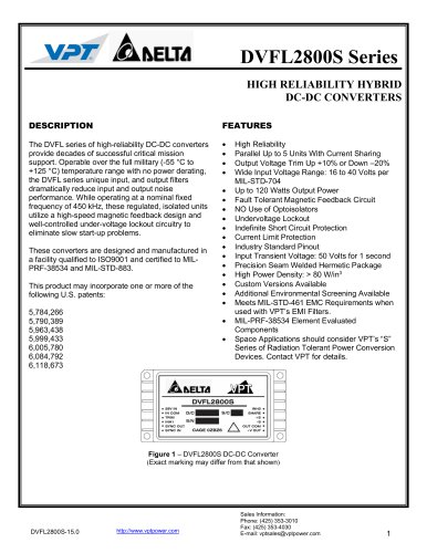
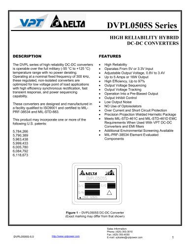
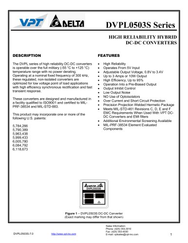
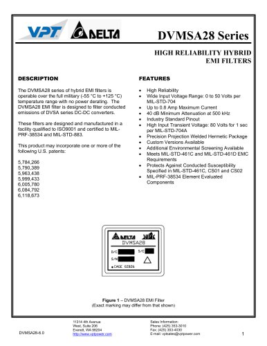
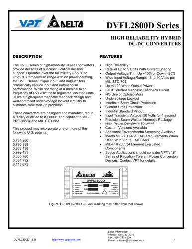
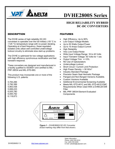
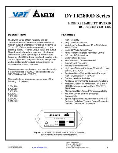
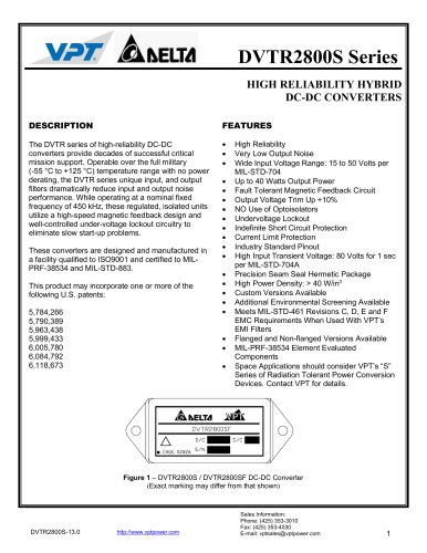
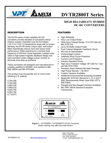
DVFL2800S Series HIGH RELIABILITY HYBRID DC-DC CONVERTERS DESCRIPTION The DVFL series of high-reliability DC-DC converters provide decades of successful critical mission support. Operable over the full military (-55 °C to +125 °C) temperature range with no power derating, the DVFL series unique input, and output filters dramatically reduce input and output noise performance. While operating at a nominal fixed frequency of 450 kHz, these regulated, isolated units utilize a high-speed magnetic feedback design and well-controlled under-voltage lockout circuitry to eliminate slow start-up problems. These converters are designed and manufactured in a facility qualified to ISO9001 and certified to MIL-PRF-38534 and MIL-STD-883. This product may incorporate one or more of the following U.S. patents: 5,784,266 5,790,389 5,963,438 5,999,433 6,005,780 6,084,792 6,118,673 FEATURES • High Reliability • Parallel Up to 5 Units With Current Sharing • Output Voltage Trim Up +10% or Down -20% • Wide Input Voltage Range: 16 to 40 Volts per MIL-STD-704 • Up to 120 Watts Output Power • Fault Tolerant Magnetic Feedback Circuit • NO Use of Optoisolators • Undervoltage Lockout • Indefinite Short Circuit Protection • Current Limit Protection • Industry Standard Pinout • Input Transient Voltage: 50 Volts for 1 second • Precision Seam Welded Hermetic Package • High Power Density: > 80 W/in3 • Custom Versions Available • Additional Environmental Screening Available • Meets MIL-STD-461 EMC Requirements when used with VPT’s EMI Filters. • MIL-PRF-38534 Element Evaluated Components • Space Applications should consider VPT’s "S” Series of Radiation Tolerant Power Conversion Devices. Contact VPT for details. Sales Information: Phone: (425) 353-3010 Fax: (425) 353-4030 E-mail: [email protected]
Open the catalog to page 1
1. Dependent on output voltage. 2. Time for output voltage to settle within 1 % of its nominal value. 4. Verified by initial electrical design verification. Post design verification, parameter shall be guaranteed to the limits specified. 5. Correction factor of 0.12 added to ceramic capacitors.
Open the catalog to page 2
1. Dependent on output voltage. 2. Time for output voltage to settle within 1 % of its nominal value. 3. Derate linearly to 0 at 135°C. 4. Verified by initial electrical design verification. Post design verification, parameter shall be guaranteed to the limits specified.
Open the catalog to page 3
1. Dependent on output voltage. 2. Time for output voltage to settle within 1 % of its nominal value. 4. Verified by initial electrical design verification. Post design verification, parameter shall be guaranteed to the limits specified. 5. Correction factor of 0.12 added to ceramic capacitors.
Open the catalog to page 4
1. Dependent on output voltage. 2. Time for output voltage to settle within 1 % of its nominal value. 3. Derate linearly to 0 at 135°C. 4. Verified by initial electrical design verification. Post design verification, parameter shall be guaranteed to the limits specified.
Open the catalog to page 5
1. Dependent on output voltage. 2. Time for output voltage to settle within 1 % of its nominal value. 4. Verified by initial electrical design verification. Post design verification, parameter shall be guaranteed to the limits specified. 5. Correction factor of 0.12 added to ceramic capacitors.
Open the catalog to page 6
1. Dependent on output voltage. 2. Time for output voltage to settle within 1 % of its nominal value. 3. Derate linearly to 0 at 135°C. 4. Verified by initial electrical design verification. Post design verification, parameter shall be guaranteed to the limits specified.
Open the catalog to page 7
1. Dependent on output voltage. 2. Time for output voltage to settle within 1 % of its nominal value. 4. Verified by initial electrical design verification. Post design verification, parameter shall be guaranteed to the limits specified. 5. Correction factor of 0.12 added to ceramic capacitors.
Open the catalog to page 8
1. Dependent on output voltage. 2. Time for output voltage to settle within 1 % of its nominal value. 3. Derate linearly to 0 at 135°C. 4. Verified by initial electrical design verification. Post design verification, parameter shall be guaranteed to the limits specified.
Open the catalog to page 9
1. Dependent on output voltage. 2. Time for output voltage to settle within 1 % of its nominal value. 4. Verified by initial electrical design verification. Post design verification, parameter shall be guaranteed to the limits specified. 5. Correction factor of 0.12 added to ceramic capacitors.
Open the catalog to page 10
1. Dependent on output voltage. 2. Time for output voltage to settle within 1 % of its nominal value. 3. Derate linearly to 0 at 135°C. 4. Verified by initial electrical design verification. Post design verification, parameter shall be guaranteed to the limits specified.
Open the catalog to page 11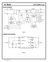
DVFL2800S Series BLOCK DIAGRAM PIN 1 UNDER VOLTAGE SHUTDOWN VOLTAGE AND CURRENT AMPLIFIERS PRIMARY HOUSEKEEPING SUPPLY SECO NDARY HOUSEKEEPING SUPPLY
Open the catalog to page 12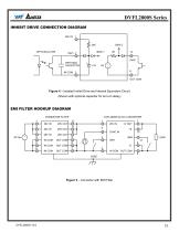
DVFL2800S Series INHIBIT DRIVE CONNECTION DIAGRAM 28V IN 1 30K OPTOISOLATOR OPTIONAL CAPACITOR Figure 4 – Isolated Inhibit Drive and Internal Equivalent Circuit (Shown with optional capacitor for turn-on delay) EMI FILTER HOOKUP DIAGRAM DVME28 EMI FILTER 1 Figure 5 – Converter with EMI Filter
Open the catalog to page 13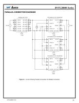
DVFL2800S Series PARALLEL CONNECTION DIAGRAMS CASE DVFL2800S DC-DC CONVERTER 1 CASE DVFL2800S DC-DC CONVERTER 1 Figure 6 – Current Sharing Parallel Connection for Multiple Converters
Open the catalog to page 14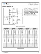
The output voltage can be trimmed down by connecting a resistor between the TRIM pin (PIN 3) and the +V OUT pin (PIN 7), or can be trimmed up by connecting a resistor between the TRIM pin (PIN 3) and the OUT COM pin (PIN 8). The maximum trim range is +10% up and -20% down. The appropriate resistor values versus the output voltage are given in the trim table below. (continued on next page)
Open the catalog to page 15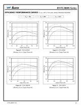
DVFL2800S Series EFFICIENCY PERFORMANCE CURVES (TCASE = 25°C, Full Load, Unless Otherwise Specified) VIN = 16V Efficiency (%) vs. Output Power (W) Efficiency (%) vs. Output Power (W) Efficiency (%) vs. Output Power (W) Efficiency (%) vs. Output Power (W)
Open the catalog to page 17All VPT INC. catalogs and technical brochures
 DVETR2800S
16 Pages
 DVEHF2800T
12 Pages
 DVPL0510S
13 Pages
 DVPL0505S
13 Pages
 DVPL0503S
12 Pages
 DVMSA28
9 Pages
 DVFL2800D
28 Pages
 DVHE2800S
15 Pages
 DVTR2800D
21 Pages
 DVTR2800S
22 Pages
 DVTR2800T
15 Pages
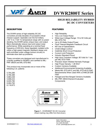 DVWR2800T
14 Pages
 DVHF2800D
17 Pages
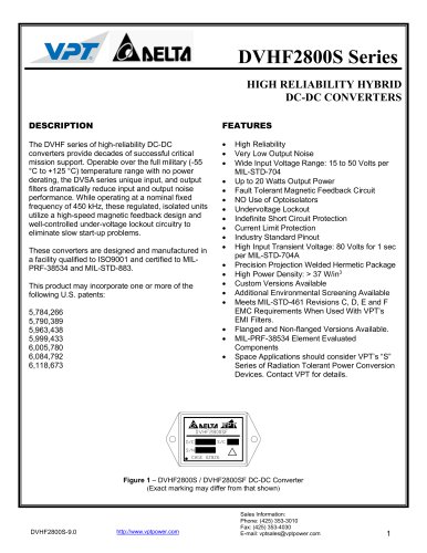 DVHF2800S
18 Pages
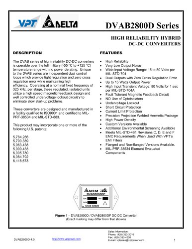 DVAB2800D
14 Pages
 DVHF+2800T
17 Pages
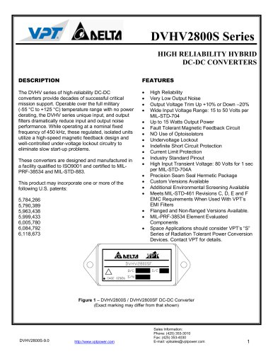
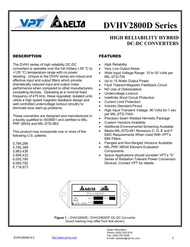 DVHV2800D
17 Pages
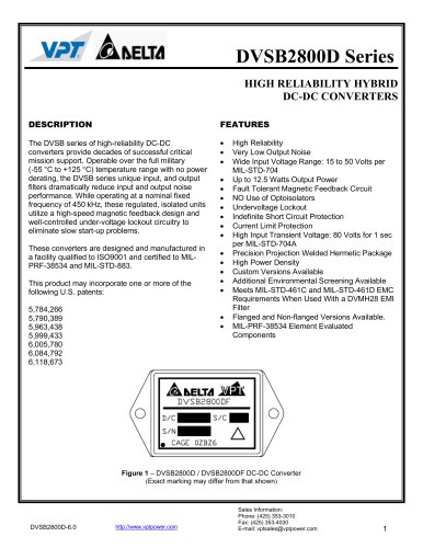 DVSB2800D
14 Pages
 DVHV2800S
17 Pages
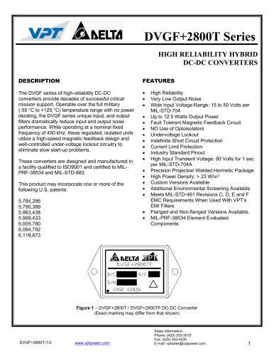 DVGF+2800T
15 Pages
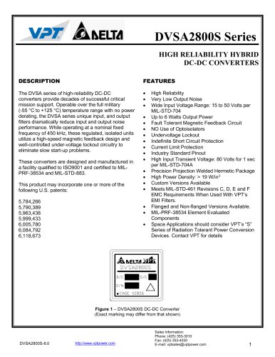
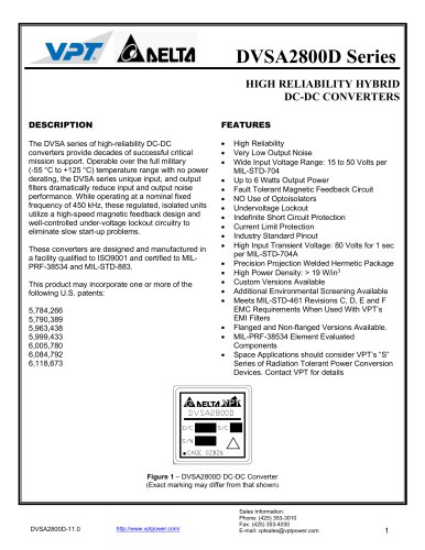 DVSA2800D
16 Pages
 DVSA2800S
15 Pages
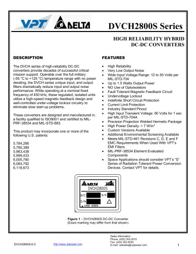 DVCH2800S
14 Pages