- Catalogs
- SURAGUS GMBH
- EddyCus® TF map 5050 series
EddyCus® TF map 5050 series

EddyCus® TF map 5050 series
- Measurement Technology: Non-contact eddy current sensor.
- Substrates: Suitable for foil, glass, wafer.
- Max Scanning Area: 20 inch / 508 x 508 mm (larger on request).
- Edge Effect Correction: 2 mm edge exclusion for standard size.
- Max Sample Thickness/Sensor Gap: 2 / 5 / 10 / 25 mm.
- Sheet Resistance Range and Accuracy: 0.001 – 10 Ohm/sq < 2% accuracy, 10 – 100 Ohm/sq < 3% accuracy, 100 – 1,000 Ohm/sq < 5% accuracy.
- Thickness Mapping: 2 nm – 2 mm for metal films.
- Scanning Pitch: 1 / 2 / 5 mm / 10 mm.
- Measurement Points: 10,000 points in 5 minutes, 1,000,000 points in 30 minutes.
- Scanning Time: 8 inch / 200 x 200 mm in 1.5 to 15 minutes, 12 inch / 300 x 300 mm in 3 to 30 minutes.
- Device Dimensions/Weight: 46.5 x 11.4 x 35.4 inch / 1180 x 290 x 900 mm / 120 kg.
Catalog excerpts
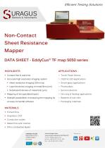
Efficient Testing Solutions Non-Contact Sheet Resistance Mapper DATA SHEET - EddyCus® TF map 5050 series HIGHLIGHTS > Touch Panel Sensor Accurate high resolution imaging system sheet resistance imaging (Ohm/sq) Layer thickness imaging of metal films (nm) Substrate thickness of metal foils (µm) Mapping of encapsulated layers > De-icing & heating applications Multiple possibilities of analyzing the mapping by > Batteries & fuel cells MATERIALS Printed films Graphene, CNT Conductive oxides Metal films and meshes Other conductive layers SURAGUS GmbH Maria-Reiche-Str. 1 01109 Dresden Germany
Open the catalog to page 1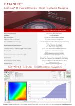
DATA SHEET EddyCus® TF map 5050 series – Sheet Resistance Mapping EddyCus® TF map 5050SR series Measurement technology Substrates Max. scanning area Edge effect correction / exclusion Max. sample thickness/ sensor gap Sheet resistance range and accuracy Thickness mapping of metal films (e.g. Aluminum, Copper) Scanning pitch Measurement points per time (quadratic shape) Scanning time Non-contact eddy current sensor e.g. foil, glass, wafer 20 inch / 508 x 508 mm (larger on request) 2 mm edge exclusion for standard size 2 / 5 / 10 / 25 mm (defined by the thickest sample/ application) 0.001 – 10...
Open the catalog to page 2All SURAGUS GMBH catalogs and technical brochures
 EddyCus® TF map 2525SR
2 Pages
 EddyCus® TF inline SR
2 Pages
 EddyCus® TF lab 4040SR
2 Pages
 EddyCus® TF lab 2020SR
2 Pages
 - EddyCus® CF inline GAP
2 Pages
 EddyCus® CF rob
2 Pages
 EddyCus® TF lab 2020
2 Pages
 EddyCus® TF inline
2 Pages
 EddyCus® TF lab 4040
2 Pages
 EddyCus® CF rob
2 Pages
 EddyCus® CF map 6060
2 Pages


- Aeronautical software
- 3D software
- 2D software
- Laser scanner
- Aeronautic laser scanner
- Non-contact laser scanner
- Thickness gauge
- Aeronautic thickness gauge
- Coating thickness gauge
- 3D laser scanner
- NDT thickness gauge
- Contact laser scanner
- Eddy current thickness gauge
- Digital display thickness gauge
- Glass thickness gauge
- Aeronautic crack detector
- Crack detector
- Film thickness gauge