- Catalogs
- SURAGUS GMBH
- EddyCus® TF map 2525SR
EddyCus® TF map 2525SR

EddyCus® TF map 2525SR
- Contact-free imaging
- High resolution imaging (25 to 1,000,000 points)
- Defect imaging
- Mapping of encapsulated layers
- Architectural glass (LowE), touch screens, flat monitors
- OLED, LED, smart-glass applications
- Transparent antistatic foils, photovoltaics, semiconductors
- De-icing, heating applications, batteries, fuel cells
- Packaging materials
- Metal thickness (nm, µm), sheet resistance (Ohm/sq), emissivity
- Conductivity/resistivity (mOhm cm), electrical anisotropy (%)
- Weight (g/m²), drying status (%), permeability (H/m) Beta
- Materials: Metal films, conductive oxides, nanowire films, graphene, CNT, graphite, printed films, conductive polymers (PEDOT:PSS)
- Non-contact eddy current sensor
- Substrates: Foils, glass, wafer
- Max. scanning area: 10 inch / 254 mm x 254 mm
- Edge effect correction/exclusion: 2 – 10 mm
- Max. sample thickness/sensor gap: 3 / 5 / 10 / 15 mm
- Thickness measurement of metal films: 2 nm – 2 mm
- Scanning pitch: 1 / 2 / 5 / 10 mm
- Measurement points per time: 100 in 0.5 minutes, 10,000 in 3 minutes
- Scanning time: 4 inch in 0.5 to 3 minutes, 8 inch in 1.5 to 15 minutes
- Device dimensions/weight: 23.6" x 9.05" x 31.5" / 27 kg
- Pre-defined measurement and product recipes
- Line scan, histogram, area analysis
- Black and colored image coding
- CSV & PDF export, SPC summary and export
- 3 user levels, material database for parameter conversion
- Edge effect compensation, storage and import of data
- Export of data sets to EddyEva, MS Excel, Origin
- VLSR (Very Low Sheet Resistance): 0.0001 – 0.1 Ohm/sq, Accuracy ± 1%
- LSR (Low Sheet Resistance): 0.01 – 10 Ohm/sq, Accuracy ± 1 – 2%
- MSR (Medium Sheet Resistance): 0.1 – 100 Ohm/sq, Accuracy ± 1 – 3%
- Repeatability (2σ): VLSR < 0.5%, LSR < 1%
Catalog excerpts

Efficient Tes�ng Solu�ons EddyCus® TF map 2525SR – Sheet Resistance Imaging Device Device Series Contact-free imaging High resolu�on imaging (25 to Sheet resistance (Ohm/sq) Defect imaging Conduc�vity / resis�vity (mOhm cm) Mapping of encapsulated layers Electrical anisotropy (%) Weight (g/m²) and drying status (%) Architectural glass (LowE) Touch screens and flat monitors Nanowire films Smart-glass applica�ons Transparent an�sta�c foils Printed films Conduc�ve polymers (PEDOT:PSS) Other conduc�ve films and materials De-icing and hea�ng applica�ons Ba�eries and fuel cells Packaging materials Visit us at: www.suragus.com www.suragus.com/calculator www.suragus.com/EddyCusMap2525 Conduc�ve oxides Metal films and meshes
Open the catalog to page 1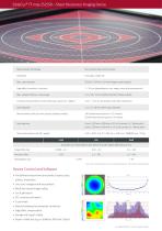
EddyCus® TF map 2525SR – Sheet Resistance Imaging Device Measurement technology Non-contact eddy current sensor Foils, glass, wafer, etc. 10 inch / 254 mm x 254 mm (larger upon request) Edge effect correc�on / exclusion 2 – 10 mm (depending on size, range, setup and requirements) Max. sample thickness / sensor gap 3 / 5 / 10 / 15 mm (defined by the thickest sample) Thickness measurement of metal films (e.g. aluminum, copper) 2 nm – 2 mm (in accordance with sheet resistance) Scanning pitch 1 / 2 / 5 / 10 mm (other upon request) Measurement points per �me (square shaped samples) 100 measurement...
Open the catalog to page 2All SURAGUS GMBH catalogs and technical brochures
 EddyCus® TF inline SR
2 Pages
 EddyCus® TF lab 4040SR
2 Pages
 EddyCus® TF lab 2020SR
2 Pages
 - EddyCus® CF inline GAP
2 Pages
 EddyCus® CF rob
2 Pages
 EddyCus® TF map 5050 series
2 Pages
 EddyCus® TF lab 2020
2 Pages
 EddyCus® TF inline
2 Pages
 EddyCus® TF lab 4040
2 Pages
 EddyCus® CF rob
2 Pages
 EddyCus® CF map 6060
2 Pages


- Aeronautical software
- 3D software
- 2D software
- Laser scanner
- Aeronautic laser scanner
- Non-contact laser scanner
- Thickness gauge
- Aeronautic thickness gauge
- Coating thickness gauge
- 3D laser scanner
- NDT thickness gauge
- Contact laser scanner
- Eddy current thickness gauge
- Digital display thickness gauge
- Glass thickness gauge
- Aeronautic crack detector
- Crack detector
- Film thickness gauge