Catalog excerpts

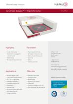
Efficient Testing Solutions SURACUS®) Sensors & Instruments 1 Data Sheet- EddyCus® TF map 5050 Series Highlights ► Contact-free imaging ► High resolution imaging (25 to 1,000,000 points) ► Defect imaging ► Mapping of encapsulated layers Applications ► Architectural glass (LowE) ► Touch screens and flat monitors ► OLED and LED applications ► Smart-glass applications ► Transparent antistatic foils ► Photovoltaics ► Semiconductors >■ De-icing and heating applications * Batteries and fuel cells t Packaging materials Parameters ► Sheet resistance (Ohm/sq) ► Metal layer thickness (nm, |um) ► Metal substrate thickness (|um) ► Anisotropy ► Defects ► Integrity assessment Materials ► Metal films and meshes ► Conductive oxides ► Nanowire films ► Graphene, CNT, Graphite ► Printed films ► Conductive polymers (PEDOT:PSS) ► Other conductive films and materials SURAGUS GmbH Maria-Reiche-StraBe 1 01109 Dresden Germany +49 35132 111520 info@suragus.com www.suragus.com www.sheet-resistance-testing.com www.suragus.com/FAQ www.suragus.com/EddyCusMap5050 Made and Engineered in Germany Innovation Award by Free State of Saxony 2013 1st Place
Open the catalog to page 1
Measurement technology Non-contact eddy current sensor 20 inch / 508 x 508 mm (larger on request) Edge effect correction / exclusion 2 - 5 mm edge exclusion for standard sizes Max. Sample thickness / sensor gap 2 / 5 / 10 / 25 mm (defined by the thickest sample) Sheet resistance range accuracy can be op�mized over sheet resistance decade within a customer specified range Thickness measurement of metal films (e.g. Aluminum, Copper) 2 nm - 2 mm (in accordance with sheet resistance) Scanning Pitch 10,000 measurement points in 5 minutes 1,000,000 measurement points in 30 minutes Scanning �me 8...
Open the catalog to page 2All SURAGUS GMBH catalogs and technical brochures
-
EddyCus® TF map 2525SR
2 Pages
-
EddyCus® TF inline SR
2 Pages
-
EddyCus® TF lab 4040SR
2 Pages
-
EddyCus® TF lab 2020SR
2 Pages
-
- EddyCus® CF inline GAP
2 Pages
-
EddyCus® CF rob
2 Pages
-
EddyCus® TF map 5050 series
2 Pages
-
EddyCus® TF lab 2020
2 Pages
-
EddyCus® TF inline
2 Pages
-
EddyCus® TF lab 4040
2 Pages
-
EddyCus® CF rob
2 Pages
-
EddyCus® CF map 6060
2 Pages


