- Catalogs
- Solitron Devices
- SD11487
SD11487

SD11487
- Superior system efficiency due to low switching and conduction losses of SiC.
- Outstanding power conversion efficiency at high frequency operation.
- High-speed switching with low capacitance.
- Reduced parasitic inductance and capacitance.
- Real Kelvin source connection for stable gate drive.
- Isolated backside for direct mount to heatsink.
- ALN substrate and CuMo baseplate for thermal conductivity.
- High junction temperature operation.
- Low junction to case thermal resistance.
- Reduced thermal requirements and system cost.
- Integrated NTC temperature sensor.
- VDS = 1200V
- RDSon = 22mΩ
- ID = 95A @ TC = 25°C
- 1: S1
- 2: G1, G2
- 3-4: Temp. Monitoring
- 5: G4, G4
- 6: S2
- 7-8: AC
- 9-10: N
- 11-12: P
- Drain-Source Voltage (VDSS): 1200V
- Continuous Drain Current (ID): 95A
- Pulsed Drain Current (ID, pulse): 237A
- Gate-Source Voltage (VGSS): -4 to 22V
- Junction Temperature (TJ, TSTG): -55 to +175°C
- Drain-Source Breakdown Voltage (V(BR)DSS): 1200V
- Off-State Drain Current (IDSS): 1-10µA
- Gate-Source Leakage Current (IGSS): ±100nA
- Gate Threshold Voltage (VGS(th)): 2.7-5.6V
- Drain-Source On-state Resistance (RDS(on)): 22-33mΩ
- Gate Input Resistance (RG): 4Ω
- Transconductance (gfs): 14.2S
- Input Capacitance (Ciss): 2879pF
- Output Capacitance (Coss): 237pF
- Reverse Transfer Capacitance (Crss): 108pF
- Effective Output Capacitance (Co(er)): 213pF
- Turn-On Delay Time (td(on)): 29ns
- Rise Time (tr): 44ns
- Turn-Off Delay Time (td(off)): 67ns
- Fall Time (tf): 28ns
- Turn-On Switching Loss (Eon): 632µJ
- Turn-Off Switching Loss (Eoff): 243µJ
- Total Gate Charge (Qg): 178nC
- Gate-Source Charge (Qgs): 40nC
- Gate-Drain Charge (Qgd): 80nC
- Gate Plateau Voltage (Vplateau): 9.6V
- Inverse Diode Continuous, Forward Current (IS): 95A
- Inverse Diode Direct Current, Pulsed (ISM): 237A
- Diode Forward Voltage (VSD): 3.2V
- Reverse Recovery Time (trr): 28ns
- Reverse Recovery Charge (Qrr): 475nC
- Peak Reverse Recovery Current (Irrm): 12A
Dimensions are provided in inches and millimeters for precise installation and integration.
Note: Specifications are subject to change without notice. Solitron Devices accepts no responsibility for errors or inaccuracies.
Catalog excerpts
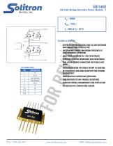
SiC Half-Bridge Hermetic Power Module - 1 VDS = 1200V RDSon = 22mΩ ID = 95A @ TC = 25°C • HIGH SPEED SWITCHING W/ LOW CAPACITANCE Temp. Monitoring Temp. Monitoring • REAL KELVIN SOURCE CONNECTION FOR STABLE GATE DRIVE • ISOLATED BACKSIDE FOR DIRECT MOUNT TO HEATSINK • ALN SUBSTRATE AND CUMO BASEPLATE FOR THERMAL CONDUCTIVITY • HIGH JUNCTION TEMPERATURE OPERATION • LOW JUNCTION TO CASE THERMAL RESISTANCE • REDUCED THERMAL REQUIREMENTS AND SYSTEM COST • INTEGRATED NTC TEMPERATURE SENSOR • REDUCED PARASITIC INDUCTANCE AND CAPACITANCE • SUPERIOR SYSTEM EFFICIENCY DUE TO LOW SWITCHING AND CONDUCTIONS LOSSES OF SIC • OUTSTANDING POWER CONVERSION EFFICIENCY AT HIGH FREQUENCY OPERATION FEATURES & BENEFITS
Open the catalog to page 1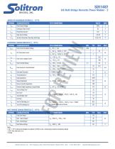
SiC Half-Bridge Hermetic Power Module - 2 ABSOLUTE MAXIMIMUM RATINGS (Ta = 25°C) Drain-Source Voltage Continuous Drain Current Pulsed Drain Current Gate-Source Voltage Junction Temperature, Operating and Storage ELECTRICAL CHARACTERISTICS (Ta = 25°C) SYMBOL V(BR)DSS lDSS IGSS+ IGSS- TEST CONDITIONS Drain-Source Breakdown Voltage Off -State Drain Current Gate-Source Leakage Current Gate Threshold Voltage Drain-Source On-state Resistance 3 Gate Input Resistance Input Capacitance Output Capacitance Reverse Transfer Capacitance Effective Output Capacitance, Energy Related Turn-On Delay Time 3 Turn-Off...
Open the catalog to page 2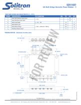
SiC Half-Bridge Hermetic Power Module - 3 BODY DIODE RATINGS AND CHARACTERISTICS (Ta = 25°C) CHARACTERISTIC Inverse Diode Continuous, Forward Current Inverse Diode Direct Current, Pulsed Diode Forward Voltage 3 Reverse Recovery Time Reverse Recovery Charge Peak Reverse Recovery Current 3 TEST CONDITIONS PACKAGE OUTLINE - dimensions in inches (mm) © 2024 Solitron Devices, Inc. This document is believed to be correct at the time of publication and Solitron Devices accepts no responsibility for consequences from printing errors or inaccuracies. All specifications are subject to change without notice....
Open the catalog to page 3All Solitron Devices catalogs and technical brochures
 SD11461
3 Pages
 SMF404
3 Pages
 SD11721
6 Pages
 SD11714
3 Pages
 SD11710
5 Pages
 SD11705
5 Pages
 2N5114 | 2N5115 | 2N5116
2 Pages
 2N5911 | 2N5912
2 Pages
 2N4416 | 2N4416A
2 Pages
 2N4391 | 2N4392 | 2N4393
2 Pages
 2N4338 | 2N4339
3 Pages
 2N4901 | 2N4902 | 2N4903
2 Pages
 2N3957 | 2N3958
2 Pages
 2N3821 | 2N3822
2 Pages
 SD11812
2 Pages
 SD11800
3 Pages
 SD11801
3 Pages
 SD11809
2 Pages
 SD11804
3 Pages
 SD11803
3 Pages

